
Lab 3 Hints and Tips for the Adder and Multiplier Circuits
The adder circuit is to be done using NAND (multiple input OK) and XOR gates ONLY! For the first part of the lab, you are to build a 4-bit adder by chaining together four full adder circuits built using NAND and XOR gates. Use the 8-position switch provided in your lab kit for input (4 positions for one number, 4 for the other), and send the output signals into a 7448 chip to drive the seven-segment display. Be sure to add an extra single LED to indicate if the two numbers add up to more than 0F (Hex) , or if you want to make it look nicer, you can set up a second 7448 and seven-segment display.
There is another bag of parts in your locker for this lab, however, all necessary parts HAVE NOT been included, only the ones not available from the electronic storeroom! Be sure to check the storeroom door for open times and check blue cabinet for circuits. You will have to obtain NAND and XOR gates from the storeroom for the adder, and a counter (74X93 or similar), a single carry register (74X74 or similar) and possibly an additional gate for the decision part (Q0=1?) of the algorithm for the multiplier. (BTW, when I say 74X00, for example, I mean 7400, 74LS00, 74S00, 74F00, etc.).
One recipe for the 4-bit adder can be implemented using:
2 74X86 Quad 2-input XOR gates
3 74X00 Quad 2-input NAND gates
2 74X10 Triple 3-input NAND gates
1 8-position switch
1 74X48 BCD to 7-Segment Decoder/Driver1 Green 7-segment LED
1 510 Ohm resistor pack (blue or white)
The parts bag for this lab contains:
1 8-position dip-switch
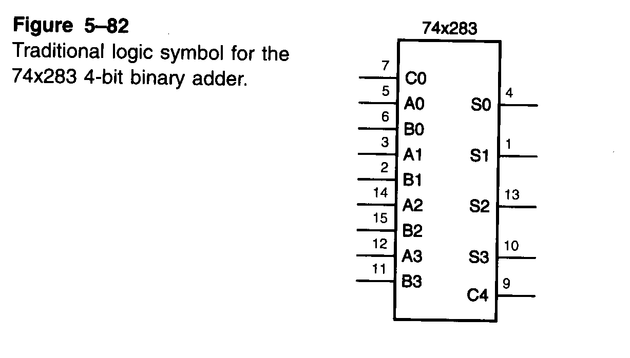
1 74LS283 Full-Adder circuit
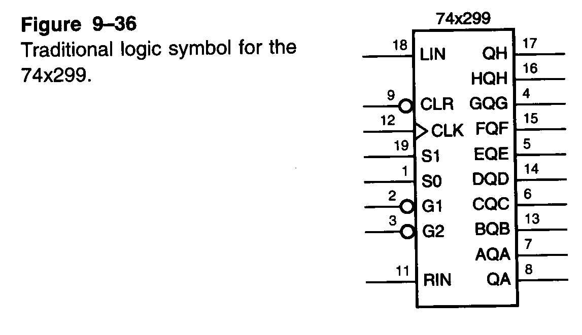
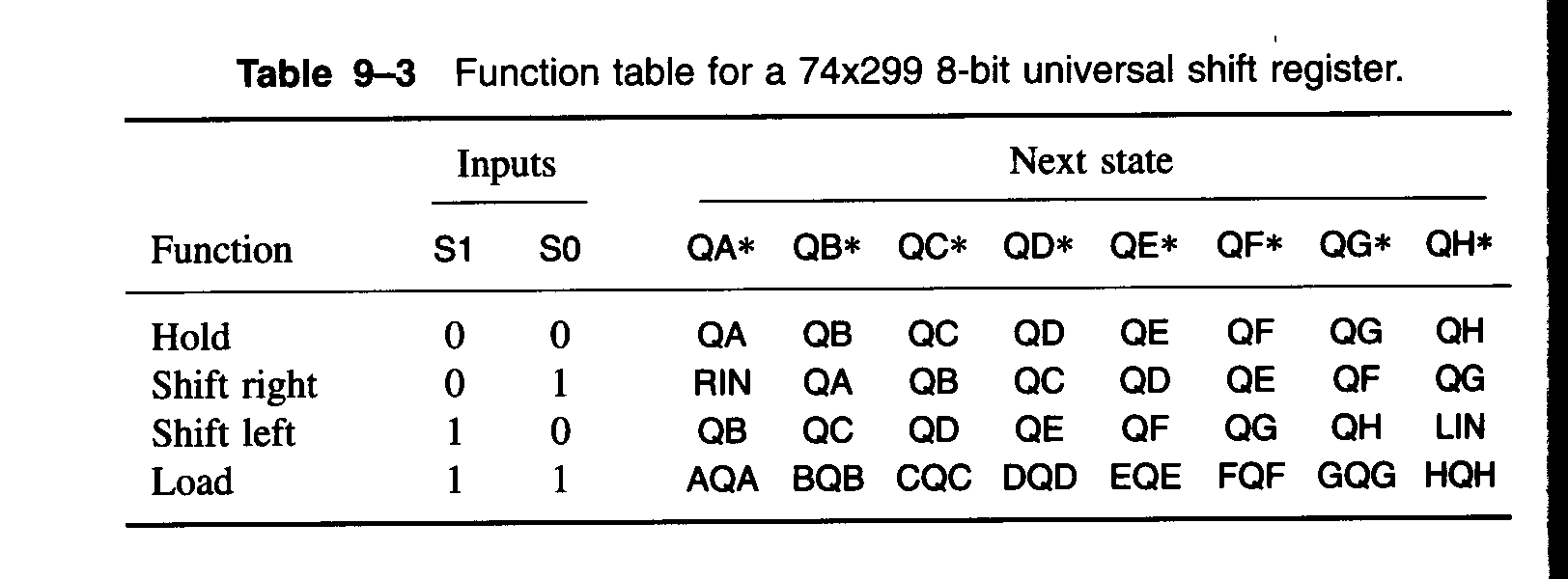
1 74LS299 Universal Shift Register
1 7448 or 74LS48 BCD to 7-Segment Decoder/Driver
1 Green 7-Segment LED with reinforced contacts
1 16-pin 510 Ohm white resistor pack (8 resistors isolated)
1 555 Timer circuit
You may use the LED circuit that you built for Lab 2 as output for the adder in Lab 3. You will need to add a second 7448 and 7-segment LED as output for the multiplier. Do not use the 74LS283 provided for the adder portion of the lab! You may use this circuit optionally if space is at a premium in the multiplier portion of the lab only, or you may simply build the multiplier using the NAND and XOR adder as the base.
Although the adder is reasonably easy to build, and may not take any more than an afternoon to build and test, do realize that the multiplier may be considerably more difficult, and make sure that you set aside enough time for experimentation and test. You may wish to use the logic analyzers in Glennan 308 to watch individual signals.
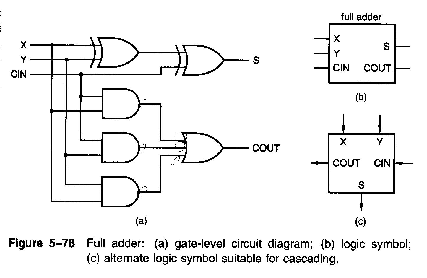
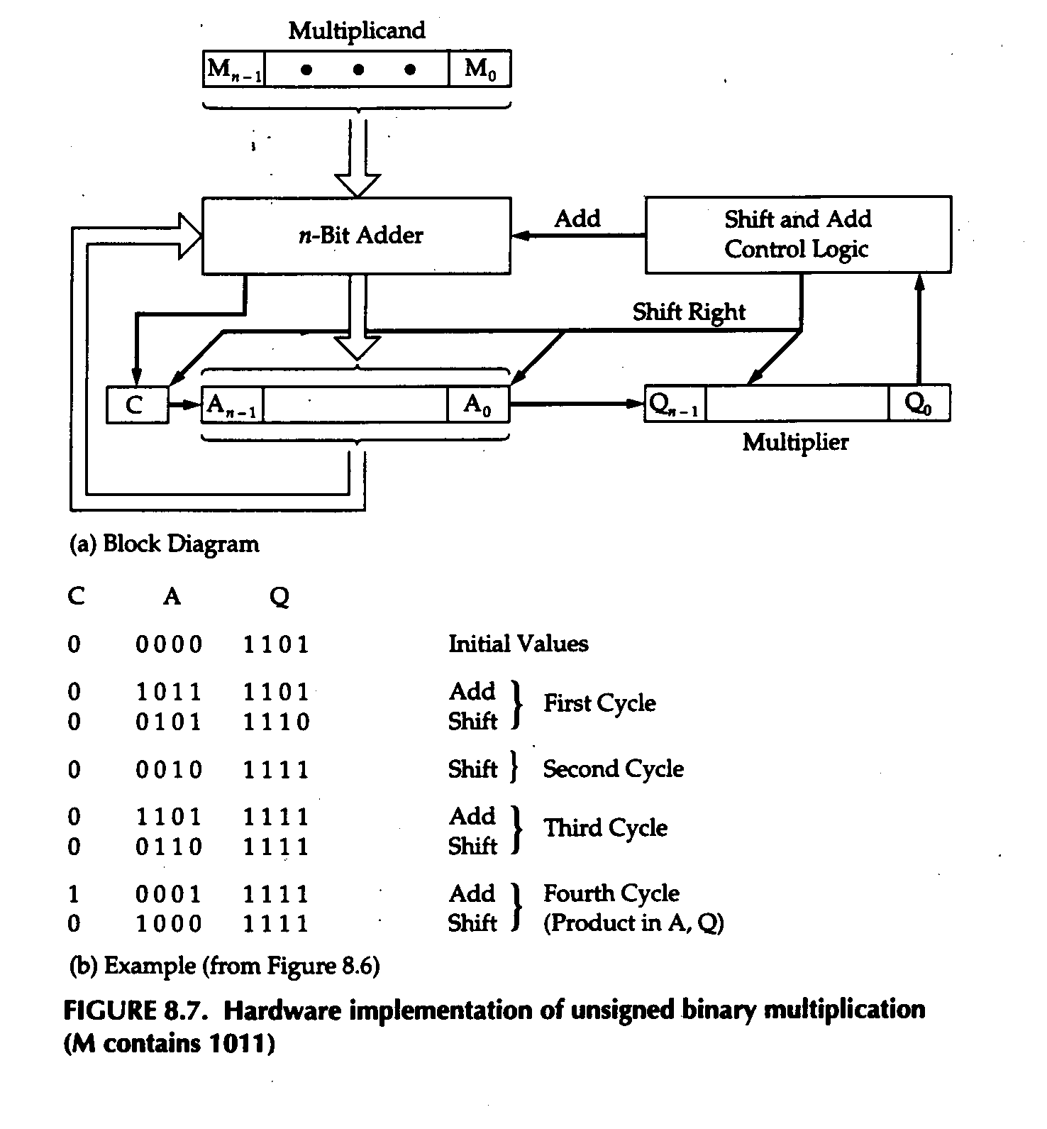
I've included a few diagrams below to assist you. The first figure, from Wakerly's Digital Design book, shows a one-stage full-adder. Use your logic equivalents and convert the AND gates to NAND gates, and the 3-input OR gate to a 3-input NAND. The multiplier diagram is from a book by Stallings, and I've included a flowchart of the algorithm that you'll be implementing along with a step-by-step number analysis. The other figures show the pin-outs and such for the 74LS283 and 74LS299 circuits. To relate circuits to the figures, you will use either the NAND and XOR 4-bit adder that you built for the first part of the lab, or the 74LS283 chip as the 'n-Bit Adder, and the 74LS299 as An-1…A0 (4-bit accumulator) and Qn-1…Q0 (4-bit Multiplier). Mn-1…M0 (4-bit Multiplicand) can be done using 4 bits of the 8-position dip switch. The 555 timer (along with a counter, etc.) form the Shift and Add Control Logic. You may want to use the other four positions of the 8-position dip to load the multiplier. You will probably want to use a 74X74 for the stand-alone single-bit carry register C. Consult Lab 2 for pin-outs and wiring of the 7448 and 7-segment green LED, and don't forget to use the resistor pack to limit the current to the segments (and avoid burnout!).
The single lines in a diagram such as FIGURE 8.7 below indicate one signal path, while double lines, such as the one from the Multiplicand to the n-Bit Adder or from the Accumulator back to the n-Bit Adder, mean that an entire group of signals, in this case a four-bit wide signal bus, is being moved as a single operation from one block to another.
If you manage to build and document both of these circuits successfully, and just have scads of time left over, you may do extra credit items BY PRIOR REQUEST ONLY! Please consult with either Chris Papachristou or Jackie Woldering to determine points.
Extra Credit
Implement a divide circuit in the fashion of the multiplier circuit. Divide one 4-bit number by another and come up with an integer result. For example, 1100/0100=0011. Show the output using the same 7-segment LED format as the adder and multiplier.
Extra-Extra-We'll fall down on our knees and worship at your feet-Credit
Use the touch-tone keypad as input to either the adder or the multiplier circuit such that I will be able to press a single digit from 0 to 9 for the first number followed by the * key to indicate the operation (plus for adder, times for multiplier), the second number in the range of 0 to 9, followed by the # key to signify the end of the operation, and then the result of the addition or multiplication will appear on the 7-segment LED's. It is not necessary that the individual numbers entered appear in the displays, but you can try. Please let us know early if you are going to attempt this Extra-Extra-Credit so that we may alert the twinkie truck and reserve a padded cell for you at the local sanitarium.