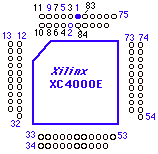
Pins of the XC4000E on the Xilinx Demo Board
Pins of the XC4003E, XC4010E and XC4005XL devices in
a 84 PLCC package
and associated connections on the Xilinx FPGA Demo Board
(Original
Document Developed At the University of Pennsylvania) and Bucknell Univ.
The following table lists the pins numbers and names for the 84 pin
XC4000 FPGA. The pins are connected to headers surrounding the socket on
the demoboard. The numbers on the demoboard headers increase from the inside
row to the outside, counter-clockwise. The corners at each header give
the starting numbers. For a description of the FPGA
Demoboard see the EE FPGA page.
After configuration, any input pin that is not used will be configured
as an input with a 50-100 kOhm pull-up resistor. Regular input pins will also
be connected to a pull-up resistor of the same value. This is done in the IOB
block on the FPGA device.
The pin numbering of the 84 pin FPGA is given in the following figure.
 |
SPECS
Device : XC4003E
No. of Logic Gates: 3,000
No. CLB: 100
fsystem freq.: 66 MHz
Delay: CLB (1.5-4.7ns, depending on the Speed grade); IOB input
2-4.8ns; IOB output (4.8-12ns). See the Xilinx data
book 2000 for more information.
XC4005XL: 5,000 logic gates; 196 logic blocks and 66MHz system
clock
Outputs can sink 12mA for the XC4000E and 3mA for the XC4000XL devices
|
|
|
Figure 1: Pin numbering of the 84 pin PLCC
|
CHIP PIN No.
|
Name
|
FPGA DEMO-BOARD Comments |
|
1
|
GND |
Ground |
|
2
|
VCC |
Power supply (5V for XC4000E and 3.5V for XC40005XL) |
|
3
|
I/O (A8) |
General I/O |
|
4
|
I/O (A9) |
General I/O |
|
5
|
I/0 (A10) |
General I/O |
|
6
|
I/O (A11) |
General I/O |
|
7
|
I/O (A12) |
General I/O |
|
8
|
I/O (A13) |
General I/O |
|
9
|
I/O (A14) |
General I/O |
|
10
|
SGCK(A15,I/O) |
General I/O |
|
11
|
VCC |
|
|
12
|
GND |
|
|
13
|
PGCK1(A16,I/O) [1] |
Clock of external oscillator (Y1) (not on all boards available);
can also used as I/O |
|
14
|
I/O(A17) |
|
|
15
|
I/O(TDI) |
XChecker TDI (Test data in) (for boundary scan, can be reused).
|
|
16
|
I/O(TCK) |
XChecker TCK (Test clock ) (for boundary scan, can be reused).
|
|
17
|
I/O(TMS) |
XChecker TMS (test mode) (for boundary scan, can be reused).
|
|
18
|
I/O |
|
|
19
|
I/O |
SW3 -1 (gen. purpose switch) |
|
20
|
I/O |
SW3 -2 |
|
21
|
GND |
|
|
22
|
VCC |
|
|
23
|
I/O |
SW3 -3 |
|
24
|
I/O |
SW3 -4 |
|
25
|
I/O |
SW3 -5 |
|
26
|
I/O |
SW3 -6 |
|
27
|
I/O |
SW3 -7 |
|
28
|
I/O |
SW3 -8 |
|
29
|
SGCK2(I/O) [2] |
7-segment disp. U7-e |
|
30
|
O(M1) |
XChecker RD/ readback, & SW2-5 ; |
|
31
|
GND |
|
|
32
|
I(MO) |
XChecker RT/readback, & SW2-4 (Mode) |
|
33
|
VCC |
|
|
34
|
I(M2) |
SW2-6 (multiple prgrm enable) |
|
35
|
PGCK2(I/O) |
7-segment disp. U7-d |
|
36
|
I/O(HDC) |
7-segment disp. U7-c; Hi untill configuration complete. Pin
is available after configuring. |
|
37
|
I/O(/LDC) |
7-segment disp. U7-dec. pt.; LO untill configuration complete;
Pin is available after configuring. |
|
38
|
I/O |
7-segment disp. U7-b |
|
39
|
I/O |
7-segment disp. U7-a, |
|
40
|
I/O |
7-segment disp. U7-f |
|
41
|
I/O(/INIT) |
7-segment disp. U8-dec. pt.; XChecker INIT |
|
42
|
VCC |
|
|
43
|
GND |
|
|
44
|
I/O |
7-segment disp. U7-g |
|
45
|
I/O |
7-segment disp. U8-e |
|
46
|
I/O |
7-segment disp. U8-d |
|
47
|
I/O |
7-segment disp. U8-c |
|
48
|
I/O |
7-segment disp. U8-b |
|
49
|
I/O |
7-segment disp. U8-a |
|
50
|
I/O |
7-segment disp. U8-f |
|
51
|
SGCK3(I/O) |
7-segment disp. U8-g |
|
52
|
GND |
|
|
53
|
DONE |
XChecker DONE |
|
54
|
VCC |
|
|
55
|
/PROGRAM |
XChecker PROG; also SW6 (Prog. switch) |
|
56
|
I/O(D7) |
SW2-7: when ON connects RST (SW4) pushbutton to pin 56 (reset
to ground). |
|
57
|
PGCK3(I/O) |
LED D13 |
|
58
|
I/O(D6) |
LED D14 |
|
59
|
I/O(D5) |
LED D15 |
|
60
|
I/O(/CS0) |
LED D16 |
|
61
|
I/O(D4) |
LED D9 |
|
62
|
I/O |
LED D10 |
|
63
|
VCC |
|
|
64
|
GND |
|
|
65
|
I/O(D3) |
LED D11 |
|
66
|
I/O(RS) |
LED D12 |
|
67
|
I/O(D2) |
|
|
68
|
I/O |
|
|
69
|
I/O(D1) |
|
|
70
|
I/O(/, RDY, /BUSY) |
|
|
71
|
I/O(D0,DIN) |
XChecker: Data IN |
|
72
|
SGCK4(DOUT,I/O) |
|
|
73
|
CCLK |
XChecker CCLK pin |
|
74
|
VCC |
|
|
75
|
O, TDO |
not connected |
|
76
|
GND |
|
|
77
|
I/O(A0,/WS) |
General I/O |
|
78
|
I/O, PGCK4(A1) |
General I/O |
|
79
|
I/O(CS1,A2) |
General I/O |
|
80
|
I/O(A3) |
General I/O |
|
81
|
I/O(A4) |
General I/O |
|
82
|
I/O(A5) |
General I/O |
|
83
|
I/O (A6) |
General I/O |
|
84
|
I/O(A7) |
General I/O |
NOTES:
1. PGCK 1-4: are primary global inputs wich drive each a dedicated internal
global net with short delays and minimal skew. If not used, each of these
pins can be a user-programmable I/O. On the demobaord PGCK1 (pin 13) can
be used for an external oscillator clock input.
2. SGCK1-4: These are four secondary global inputs. . If not used, each
of these pins can be a user-programmable I/O.
Reference:
The Programmable Logic Data Book, Xilinx, San Jose, 1997.