The SPICE dc model32,33 uses a
further simplification of the expression for IDsat given in
Eq. (5.125). First,
VT=Vbi-Vp from Eq. (5.106)
is used to eliminate Vbi in Eq. (5.125):
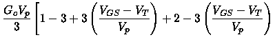
![\begin{displaymath}
I_{D_{sat}}=\frac{G_oV_p}{3}\left[ 1-\frac{3(V_p+V_T-V_{GS})}{V_p}+2\left(\frac{
V_p+V_T-V_{GS}}{V_p}\right)^{3/2}\right].
\end{displaymath}](man_spice3_jfet_img35.gif) |
(5.128) |
The
 term may be written as
2[1-(VGS-VT)/Vp]3/2 and
expanded in a three term binomial series to give
term may be written as
2[1-(VGS-VT)/Vp]3/2 and
expanded in a three term binomial series to give
![\begin{displaymath}
2\left[1-\left(\frac{V_{GS}-V_T}{V_p}\right)\right]^{3/2}=2\...
...1}{2}\frac{1}{2}\left(
\frac{V_{GS}-V_T}{V_p}\right)^2\right].
\end{displaymath}](man_spice3_jfet_img37.gif) |
(5.129) |
Equation (5.128) now becomes
| IDsat |
= |
 |
|
| |
|
![$\displaystyle \left . +\frac{3}{4}\left(\frac{V_{GS}-V_T}{V_p}\right)^2\right]
.$](man_spice3_jfet_img39.gif) |
(5.130) |
Cancellation of common terms gives
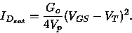 |
(5.131) |
Previously Go was given in Eq. (5.113) as
 ,
and Vp was
given in Eq. (5.104) as
,
and Vp was
given in Eq. (5.104) as
 .
Then,
.
Then,
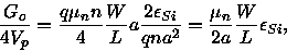 |
(5.132) |
or
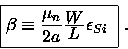 |
(5.133) |
Equations (5.131) and (5.133) may be combined to give
 |
(5.134) |
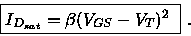
Equation (5.134) is a commonly used approximation for the JFET.
In the saturation region, the depletion region near the drain will increase
as VDS exceeds VDsat. This maximum in the depletion
depth [see Fig. 5.28 (b)] will move toward the source
and effectively shortens the channel length L much like the Early
voltage effects in bipolar junction transistors. This effect is called
channel length modulation
and is represented by the parameter
 .
The SPICE representation becomes
.
The SPICE representation becomes
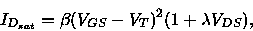 |
(5.135) |
where  is related to the output conductance given by
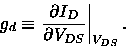 |
(5.136) |
| Table 5.3. SPICE2 or PSpice JFET Model Parameters |
|
|
Text |
SPICE |
|
Default |
|
|
No. |
Symbol |
Keyword |
Parameter Name |
Value |
Units |
|
1 |
VT |
VTO |
threshold voltage |
-2 |
V |
|
2 |
 |
BETA |
transconductance parameter |
10-4 |
A/V2 |
|
3 |

|
LAMBDA |
channel-length modulation |
0 |
V-1
|
|
4 |
RD |
RD |
drain ohmic resistance |
0 |

|
|
5 |
RS |
RS |
source ohmic resistance |
0 |
 |
| hline
6 |
CGS |
CGS |
zero-bias gate-source capacitance |
0 |
F |
|
7 |
CGD |
CGD |
zero-bias gate-drain capacitance |
0 |
F |
|
8 |
Vbi |
PB |
gate built-in potential |
1 |
V |
|
9 |
Is |
IS |
gate saturation current |
10-14 |
A |
|
10 |
FC |
FC |
coefficient for forward-bias depletion capacitance
|
0.5 |
|
|
11 |
kf |
KF |
flicker-noise coefficient |
0 |
|
|
12 |

|
AF |
flicker-noise exponent |
1 |
|
The SPICE2 or PSpice parameters for the JFET are given in Table 5.3 and have
been described by Massobrio and Antognetti.33
The optional parameters (PAR1, PAR2, )
are represented by the SPICE2
Keywords. For example, if no value is given for the
threshold voltage, the default value of -2 V will be used.
It should be noted that VT, as given by Eq. (5.107), is
related to the pinchoff voltage Vp which depends on the carrier
concentration and thickness a of the conducting layer. The next parameter
is BETA which was given in Eq. (5.133) and contains the gate width W
and length L. LAMBDA, the channel-length modulation parameter, was
introduced in Eq. (5.135).
)
are represented by the SPICE2
Keywords. For example, if no value is given for the
threshold voltage, the default value of -2 V will be used.
It should be noted that VT, as given by Eq. (5.107), is
related to the pinchoff voltage Vp which depends on the carrier
concentration and thickness a of the conducting layer. The next parameter
is BETA which was given in Eq. (5.133) and contains the gate width W
and length L. LAMBDA, the channel-length modulation parameter, was
introduced in Eq. (5.135).
The source and drain resistances, RS and
RD, represent the IR drop between the source and drain contacts and
the conducting channel. These resistances cause the experimentally
measured gm to be less than the actual channel transconductance.34
The gate-source capacitance and
gate-drain capacitances, CGS and CGD, are either
experimentally determined or estimated as described in Ref. 35. The
built-in potential PB for the p-n junction gate was given in
Eq. (4.60) and the p-n junction gate saturation current IS
is the diffusion saturation current given in Eqs. (4.115) and (4.116).
The coefficient for forward-bias depletion capacitance FC
is the same as for the p-n junction SPICE parameters in Table 5.1.
The noise parameters
are also the same as for the p-n junction in Table 5.1.
In circuit applications, the manufacturer would be
expected to provide  ,
and IS for a particular fabrication
process. The SPICE
large-signal model equivalent circuit
for the n-channel JFET is shown in Fig. 5.32.
,
and IS for a particular fabrication
process. The SPICE
large-signal model equivalent circuit
for the n-channel JFET is shown in Fig. 5.32.
Figure 5.32:
SPICE2 large-signal model equivalent circuit for the n-channel JFET (
Ref. 35).
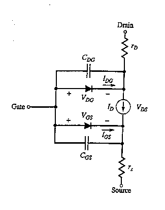 |
The two diodes represented in the equivalent circuit by IGS and
IDS are given by36
![\begin{displaymath}
I_{GS}=I_S[\exp(qV_{GS}/kT)-1],
\end{displaymath}](man_spice3_jfet_img58.gif) |
(5.137) |
and
![\begin{displaymath}
I_{DS}=I_S[\exp(qV_{DS}/kT)-1].
\end{displaymath}](man_spice3_jfet_img59.gif) |
(5.138) |
A small conductance, GMIN=10-12 mho,
is connected in parallel with IGS and
IDS as VGSGMIN and VDSGMIN to aid in convergence.
The capacitances CGS and CGD are represented by35
 |
(5.139) |
and
![\begin{displaymath}
C_{GS}=[C_{GS}(0)]/{\tt F}_2({\tt F}_3+mV_{GS}/V_{bi})~{\rm for}~V_{GS}\geq
{\tt FC}\times V_{vi}.
\end{displaymath}](man_spice3_jfet_img61.gif) |
(5.140) |
The parameters F2 and F3 are given as35
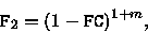 |
(5.141) |
and
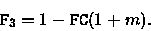 |
(5.142) |
In SPICE2 or PSpice, the grading parameter m is 0.5 and cannot be varied.
The additional optional parameters given in PSpice are
listed in Table 5.4.32,37
Parameters no. 13 - 16 are the same as for the p-n junction given in
Tables 5.1 and 5.2.
Parameters no. 17 and 18 are for the impact ionization (avalanche)
current for
0,(VGS-VT)<VDS in the saturation region which is
given as38
![\begin{displaymath}
I_i=I_{DS}\times {\tt ALPHA}\times[V_{DS}-(V_{GS}-V_T)]\times
\exp\{{\tt VK}/[V_{DS}-(V_{GS}-V_T)]\}.
\end{displaymath}](man_spice3_jfet_img64.gif) |
(5.143) |
Parameter no. 20 gives the temperature dependence of the threshold
voltage as
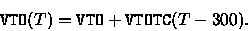 |
(5.144) |
The temperature dependence of  is given as
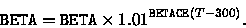 |
(5.145) |
The temperature dependence of IS, ISR, PB, CGS
and CGB are the same as for the p-n junction.
| Table 5.4. Additional PSpice JFET Model Parameters |
|
|
Text |
SPICE |
|
Default |
|
|
No. |
Symbol |
Keyword |
Parameter Name |
Value |
Units |
|
13 |
n |
N |
ideality factor |
1.0 |
-- |
|
14 |
-- |
XTI |
saturation current temperature exponent |
3.0 |
-- |
|
15 |
Isscr or Issr |
ISR |
space-charge recombination
or surface-recombination saturation current |
0 |
A |
|
16 |
n |
NR |
ideality factor |
2.0 |
-- |
|
17 |
-- |
ALPHA |
ionization coefficient |
0 |
V-1 |
|
18 |
-- |
VK |
ionization ``knee'' voltage'' |
0 |
V |
|
19 |
m |
M |
gate p-n junction grading coefficient |
0.5 |
--
|
|
20 |
-- |
VTOTC |
VTO temperature coefficient |
0 |
V/ C
-1 C
-1 |
|
21 |
-- |
BETATCE |
 exponential temperature coefficient
 |
0 |
 C C |
See also for more information
Craig Casey, Jr.
hcc@ee.duke.edu